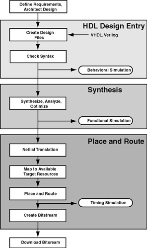
Rapid System Prototyping with FPGAs

The design implementation, phase is a significant percentage of the overall design cycle. It is critical that the implementation phase of the design be handled as efficiently as possible. The decisions before and during the design implementation phase can have a dramatic impact on the implemented design and project schedule. The "pay now or pay later" principle applies in full force during the FPGA design implementation phase. It is important to spend extra time and effort on the tasks that will ripple through and influence later design phases. The most: important design implementation tasks are presented in this chapter. Figure 7.1 presents a high-level design implementation flow.
The following definitions describe the main steps of an FPGA design's implementation phase.
Design Architecture Defining the structure, interfaces and relationships between system functional blocks. Different architectural styles such as hierarchical or flat design organization can be used to implement a design.
Design Entry Entering a design in an HDL (VHDL or Verilog). Designs may also be entered in MATLAB , Simulink , C, or C++ if the team has access to appropriate tools. However, designs described by these alternative design entry approaches will generally be translated to RTL-level VHDL/Verilog in an intermediate design step. This design phase may also be referred to as design capture.
Logic Synthesis Tool-driven process for converting VHDL/Verilog code to a gate-level netlist specific to a target device.
Place and Route Tool-driven process that determines...