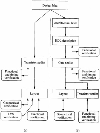
Logic-Timing Simulation and the Degradation Delay Model

Carlos Jes s Jim nez Fern ndez Manuel Valencia Barrero
The design process of VLSI integrated circuits has different options and many stages. In general, there are great differences between the design process of analog and digital integrated circuits. Figure 1.1 outlines these design processes. In every design process, the tasks to test the correctness of the design are as important as the design itself. The sooner failures are detected, the sooner failures are corrected, and the sooner and less expensive it will be to make those possible corrections.
In general, the starting point for an analog design is a circuit at the transistor level. Although in some cases it is useful to start off with functional descriptions composed of blocks of higher level (mainly amplifiers of different types), it is always necessary to extract the characteristics of these blocks and their design with transistors. Once the description of the circuit has been obtained at the transistor level, it is necessary to verify it.
The layout design is usually manual, following a methodology called full-custom. The verification of the correctness of a layout is divided into three main areas. First of all, the verification of construction rules for layout imposed by the foundry, DRC (Design Rule Check). Secondly, it must be verified that the devices implemented by the layout exist within the netlist of transistors, LVS (Layout versus Schematic). And thirdly, it must be verified that the functional behaviour...