Mosfet Modeling for Circuit Analysis and Design
The MOS structure, consisting of a metal-oxide (SiO 2)-semiconductor (Si) sandwich, made the fabrication of the first practical surface field effect transistor possible in 1960, and until now it is the core structure of Very Large Scale Integration (VLSI) systems.
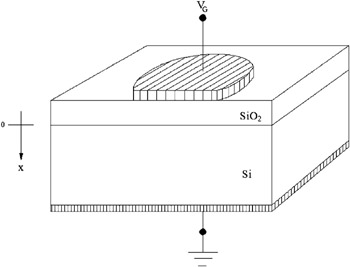
The MOS structure (Fig. 2.4) functions as a two-terminal capacitor in which a metal plate is separated from the semiconductor substrate by a thin insulator of a thermally grown SiO 2 layer. The unique properties of the SiO 2-Si system are the reduced amount of interface traps and the high dielectric strength of the SiO 2 [9]. The most common metal plate materials are aluminum and heavily doped polycrystalline silicon (polysilicon or poly). A second metal layer along the back provides an electrical contact with the silicon substrate.
The ideal MOS structure has the following properties [10]: (1) the metal gate is equipotential; (2) the oxide is a perfect insulator with zero transport current and no charge inside it or at its interfaces; (3) there are no interface traps at the SiO 2-Si interface; (4) the semiconductor is uniformly doped; (5) the semiconductor is sufficiently thick so that a field free region ( bulk ) exists far from the interface; (6) the back gate contact is ideal (ohmic); (7) the structure is one-dimensional, i.e., the electric field lines are perpendicular to the surface; and (8) the potential contact between the metal and semiconductor...