Mosfet Modeling for Circuit Analysis and Design

This appendix summarizes the basic properties of the pn junctions that are relevant to the intrinsic MOS transistor. Thus, the current-voltage and capacitance-voltage characteristics of the pn junction are not addressed here. We focus on the pn junction as a contact with the inversion layer; therefore, only the electrostatics of the junction necessary to establish the boundary conditions for the inversion channel is reviewed.
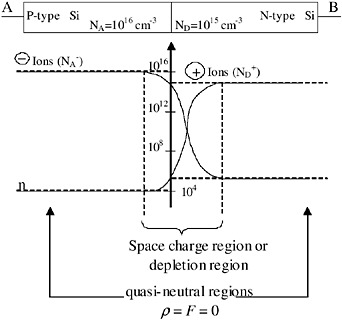
A pn junction is present when a transition between p-type and n-type doping occurs in adjacent regions of a semiconductor (crystal). Junctions are called abrupt when the transition from the p-type to the n-type doping is very narrow. The doping profile and the carrier densities of an abrupt junction, with constant doping densities on either side of the junction, are shown in Fig. E.1. As a consequence of the carrier concentration differences between the p-type and n-type regions, electrons (holes) diffuse from the n (p) side to the p (n) side, leaving behind ionized donor (acceptor) atoms and, consequently, a charge imbalance and a net charge density. The space charge region near the metallurgical junction where the mobile carrier concentrations have been reduced below their values far from the junction is called the depletion region. Far from the metallurgical junction, neutrality prevails as shown in Fig. E.1. The electric field produced by the charge imbalance counteracts the diffusion current so that in thermal equilibrium the electron and hole currents are zero. Setting the total electron current to zero yields