Wideband Amplifier Design

What else can be done? If possible, one could lower the inductance. This can be difficult because the inductance is usually a stray element. Going from a discrete design to an integrated circuit can help a lot. Placing discrete devices on a hybrid can also work wonders. Short of that, use the best possible low-inductance package. It goes without saying that trace length on the PCB should be short and carefully controlled.
One could lower the f t of the device. If the circuit does not require a high-speed transistor, do not use one! f t can also be reduced by increasing C jc. This can be done by externally adding additional capacitance.
The problem with lowering f t or increasing the base resistance, R b, is that both techniques lower the speed of the circuit. This is usually not desirable. Lowering L is the most desirable solution so far, but it may not be possible. Are there circuit techniques that can help?
The original model for this circuit is shown in Figure 2-12.
Equation (2.14) shows Z in for this network to be
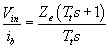
If we now assume that
| (2.61) | |
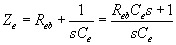
where R eb is the emitter resistance of the transistor and C e is the external capacitance, the circuit is driving.
Combining Z e with the equation for Z in