Wideband Amplifier Design

2.11: PACKAGE PARASITICS

2.11 PACKAGE PARASITICS

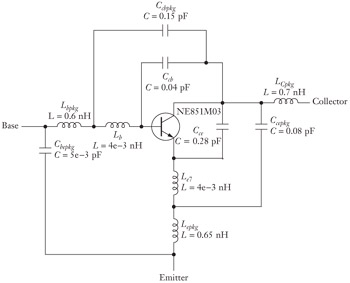
So far, we have looked at the sample circuit only as a chip; if it is in a package, then it is going to be surrounded by stray elements (particularly lead inductance) that limit what we can do. In this section, we will look at this issue. The manufacturer specifies the package parasitics for the NE851M03 as shown in Figure 2-77. Of the components shown, the dominant elements for an emitter-follower circuit are the lead inductances, L Bpkg and L Epkg, C cbpkg and C ce. L Cpkg is of concern because it raises the impedance in the collector, preventing it from being at AC ground. This could cause some additional amplification of parameters like C jc because of Miller effects. Fortunately, most of these elements are easily handled in our modeling. L Bpkg simply adds to the external inductance already modeled. For series peaking, it will simply reduce the required value of the series peak inductance. Unfortunately, its presence will prevent the use of T-coil peaking.


Figure 2-77: The NE851M03 with package strays as specified by the manufacturer.

L B is so small that for most applications it can be neglected, and C cb can be added directly to C cbpkg. Using Miller's theorem, the combined capacitor can be referred to ground from node 3. If R bb is small enough, a reasonable assumption would be to combine this capacitor with C j, the...

UNLIMITED FREE
ACCESS
TO THE WORLD'S BEST IDEAS

SUBMIT
Already a GlobalSpec user? Log in.

This is embarrasing...

An error occurred while processing the form. Please try again in a few minutes.

Customize Your GlobalSpec Experience

Category: Inductance Standards and Decades
Finish!
Privacy Policy

This is embarrasing...

An error occurred while processing the form. Please try again in a few minutes.