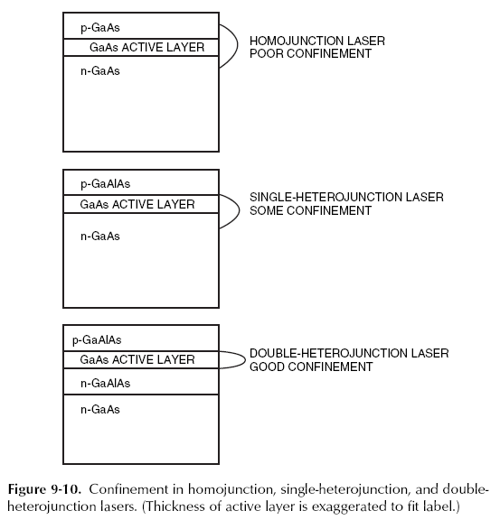
"For Credible Lasers, See Inside."
THE LASER IS LESS THAN three years younger than the space age. Just days after the Soviet Union launched Sputnik I on October 4, 1957, Charles Townes and Gordon Gould had two crucial discussions at Columbia University about the idea that would become the laser. As the United States and Soviets launched the space race, Townes and Gould went their separate ways and started their own race to make the laser. On May 16, 1960, Theodore Maiman crossed the laser finish line, demonstrating the world s first laser at Hughes Research Laboratories in California.
Bright, coherent, and tightly focused, laser beams were a new kind of light that excited the imagination. Science fiction writers turned their fictional ray guns into lasers with a stroke of the pen. Science writers inhaled deeply of the technological optimism of the early 1960s and wrote breathless predictions about the future of "the incredible laser." An article in the November 11, 1962 issue of the Sunday newspaper supplement This Week revealed U.S. Army schemes for equipping soldiers with a "death-ray gun . . . small enough to be carried or worn as a side-arm." It quoted Air Force Chief of Staff Curtis E. LeMay predicting that ground-based lasers could zap incoming missiles at the speed of light.
The reality was something else. A bemused Arthur Schawlow, who had worked with Townes on the laser, posted a copy of "The Incredible Laser" on his door at Stanford University, along with a note that read, "For credible lasers, see inside." Irnee D Haenens, who had helped Maiman make the first laser, called the laser "a solution looking for a problem," a joke that summed up the real situation. The infant laser had tremendous potential, but it had to grow up first.