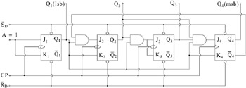
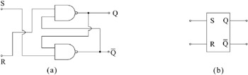
Digital Circuit Design with an Introduction to CPLDs and FPGAs

Figure 8.21(a) shows a basic Set-Reset (SR) flip flop constructed with two NAND gates, and Figure 8.21(b) shows the symbol for the SR flip flop where S stand for Set and R for Reset.
We recall that for a 2-input NAND gate the output is logical 0 when both inputs are 1s and the output is 1 otherwise. We denote the present state of the flip flop as Q n and the next state as Q n +1, with reference to Figure 8.1(a) we construct the following characteristic table.
The characteristic table of Table 8.1 shows that when both inputs S and R are logic 0 simultaneously, both outputs Q and Q are logic 1 which is an invalid condition since Q and Q are complements of each other. Therefore, the S=R=0 condition must be avoided during flip flop operation with NAND gates. When R=1 and S=0, the next state output Q n+1 becomes 0 regardless of the previous state Q n and this is known as the reset or clear condition, that is, whenever Q=0 we say that the flip flop is reset or clear. When R= 0 and S=1, the next state output Q n+1 becomes 1 regardless of the previous state Q n and this is known as the preset or simply set condition, that...