Bill asks Ted, "Do you have a final schematic of the final chip, because that's what I need to work on now."
Ted says, "Not quite yet, but I do have a schematic of one of the corners with all the pads and the ESD devices on it. But you'll probably want that as a schematic to work to anyway because there are four of these and we want them all to be identical. So having a schematic of just one corner makes your life easy."
"Yes," says Bill. "That's really useful."
Bill is given the following schematic.
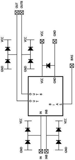 Figure CS1-58: Schematic of corner.
 Ted begins to explain the schematic to Bill. "I have added ESD diodes to the inputs and the outputs. There are also ESD diodes across the power and ground rails."
Bill says, "Um. I'm not really familiar with the analog ESD protection scheme that you're talking about there. Can you explain it a bit more?"
"Sure," says Ted.
Ted draws a box to represent his circuit and diode symbols to represent the ESD diodes.
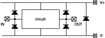 Figure CS1-59: ESD diode protection, in both directions, on every pin.
 He continues, "What we're trying to do here is protect every pin to every other pin. When someone picks up this chip with their hand, they could cause a static zap that could destroy everything. So, we want to give the zap an easy path to run through instead of running through our circuit.
"We have no idea...