Operation and Modeling of the MOS Transistor

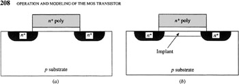
In the previous chapter, we assumed that the transistors we considered had a uniform substrate, as indicated in Fig. 5.1a. In real devices this assumption does not hold; the substrate doping is locally changed in the region between the source and the drain, as shown in Fig. 5.1b. This is achieved through ion implantation, a process in which the substrate is bombarded with ions during fabrication. The effective substrate doping concentration is changed in the areas where these ions land, and thus the substrate concentration varies as one goes from the surface toward the bulk. [ ] A main aim of this is to set the threshold voltage of transistors to a desired value, but channel implantation is also used to modify other characteristics (notably the punchthrough behavior).
Since its early application to MOS transistors, [1] [2] [3] [4] ion implantation has been used extensively and is currently a standard part of device fabrication. [5] [6] [7] [8] Ion implantation is used for more than doping the channel; for example, in Chap. 1 we encountered its use in forming the source and drain regions. [2] nMOS devices like the ones in Fig. 5.1 are formed by using ion implantation to dope the source and drain regions n +; during this process, the polysilicon gate acts as a mask, preventing the ions from landing in the channel area. In...