Operation and Modeling of the MOS Transistor

Appendix I: General Analysis of the Three-Terminal MOS Structure

Overview

For the two-terminal MOS structure on a p-type substrate the electron concentration at y was given by (2.4.13). According to the discussion in Sec. 3.2, this equation can be converted to one valid for the p-substrate three-terminal MOS structure of Fig. 3.1c by replacing ?( y) by ?( y) ? V CB.


Assuming that the holes do not communicate directly with external source in the sense discussed in Sec. 3.2 for electrons, [1], [2] [ ] their concentration will depend only on ?( y), as was the case in (2.4.14) for the two-terminal structure:


The above two equations have also been derived and discussed by using energy band concepts in Appendix H. Proceeding now as in Appendix F, we obtain Poisson's equation as follows:


Following the procedure outlined in Appendix F, the solution of the above equation leads to the following results:


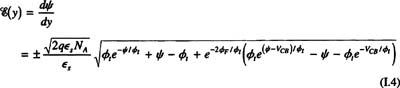
where is given by the right-hand side of (I.4).

[1]H. C. Pao and C. T. Sah, "Effects of diffusion current on characteristics of metal-oxide (insulator) semiconductor transistors," Solid-State Electronics, vol. 9, pp. 927 937, 1966.

[2]S. M. Sze, Physics of Semiconductor Devices, John Wiley, New York, 1981.

[ ]This assumption is not exactly valid because both holes and electrons are responsible for the minute reverse-bias current mentioned in Sec. 3.2.

INVERSION

For the inversion region, proceeding as in Appendix F we obtain:


Deleting negligible terms in (I.5) and using (2.5.2) and (3.2.5a)...

UNLIMITED FREE
ACCESS
TO THE WORLD'S BEST IDEAS

SUBMIT
Already a GlobalSpec user? Log in.

This is embarrasing...

An error occurred while processing the form. Please try again in a few minutes.

Customize Your GlobalSpec Experience

Category: Metal-Oxide Semiconductor FET (MOSFET)
Finish!
Privacy Policy

This is embarrasing...

An error occurred while processing the form. Please try again in a few minutes.