Operation and Modeling of the MOS Transistor

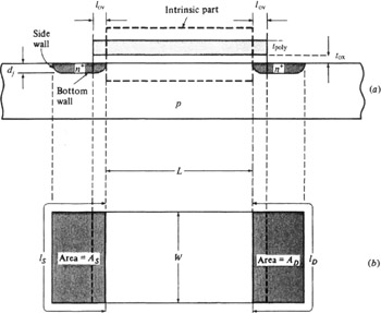
The "extrinsic" part of a transistor is everything outside the broken line in Fig. 8.27a. In this figure and in the top view in Fig. 8.27b we show some symbol definitions to be used in the following discussion.
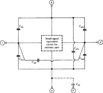
The charge storage effects associated with the extrinsic part can be modeled by using six small-signal capacitances (one between each pair of terminals), as shown in Fig. 8.28. In the symbols used for these capacitances, the first two subscripts indicate the associated device terminals and the subscript e stands for extrinsic. If the transistor happens to be inside a well on a CMOS chip (Sec. 1.6), then one must consider also the capacitance due to the pn junction between the well and the common substrate on which the well has been formed. This capacitance is denoted by C bb ? in Fig. 8.28, with b corresponding to the transistor's body and b ? corresponding to the common chip substrate. The dotted box represents the model of the intrinsic part, which has already been discussed in the previous two sections. We now concentrate on the seven extrinsic capacitances. Each of these can easily be associated with parts of the physical transistor structure, as discussed below.
GATE CAPACITANCES. Capacitances C gse and C