Operation and Modeling of the MOS Transistor

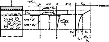
Figure E.1 shows the results of applying the basic laws of electrostatics given in Appendix B to the two-terminal MOS structure discussed in Chap. 2. The figure is based on three simplifying assumptions:
The depletion region has a uniform charge density and is assumed to contain only ionized acceptor atoms, and the region's bottom edge is sharply defined, with the semiconductor being neutral below it (depletion approximation).
The charges on the gate and at the interface are contained in extremely thin layers. The integral under the corresponding portions of the charge density plot (i.e., the corresponding charge per unit area) is Q ? G and Q ? o, respectively, as shown.
The inversion layer is much thinner than the depletion region. For simplicity, we assume that the charge density ?( y) is constant in the inversion layer. The latter assumption is not valid in practice. However, it can be seen from the material in Appendix B that, as the thickness of the inversion layer is allowed to approach zero (charge sheet model), the details of the shape of ?( y) in it become irrelevant anyway. All that counts, then, is the corresponding integral of the inversion layer charge density, which in Fig. E.1 has been denoted by Q ? I.
E. H. Nicollian and J. R. Brews, MOS Physics and Technology, John Wiley, New York, 1982.
S. M. Sze, Physics of Semiconductor Devices, John...