VHDL: Programming By Example, Fourth Edition
No matter what your current level of expertise, nothing will have you writing and verifying concise, efficient VHDL descriptions of hardware designs as fast or as painlessly as this classic tutorial.
In the last few chapters, we have discussed VHDL language features and the VHDL synthesis process. In the next few chapters, we tie all of these ideas together by developing a top-down design for a small CPU design, verify its functionality, verify that it can be synthesized, and implement the design in an FPGA device.
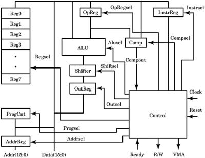
The example is a small, 16-bit microprocessor. A block diagram is shown in Figure 12-1.
The processor contains a number of basic pieces. There is a register array of eight 16-bit registers, an ALU (Arithmetic Logic Unit), a shifter, a program counter, an instruction register, a comparator, an address register, and a control unit. All of these units communicate through a common, 16-bit tristate data bus.
The top-level design consists of the processor block and a memory block communicating through a bidirectional databus, an address bus, and a few control lines. The processor fetches instructions from the external memory and executes these instructions to run a program. These instructions are stored in the instruction register and decoded by the control unit. The control unit causes the appropriate signal interactions to make the processor unit execute the instruction.
If the instruction is an add of two registers, the control unit would cause the first register value to be written to register OpReg for temporary storage. The second register value would then be placed on the data bus. The ALU would be placed in add...