VHDL: Programming By Example, Fourth Edition
No matter what your current level of expertise, nothing will have you writing and verifying concise, efficient VHDL descriptions of hardware designs as fast or as painlessly as this classic tutorial.
Throughout the book so far we have discussed a number of techniques for implementing VHDL designs and ways to make sure that the VHDL designs behave as expected. These techniques include simulation, synthesis of the design to an FPGA or ASIC, and gate-level simulation using VITAL libraries. A new technique called At-Speed Debugging is just becoming available that allows much higher performance verification than a typical simulator, yet provides the design visibility necessary to properly debug a design. This technique provides designers with the ability to debug their design in the target system, at target speed, at the VHDL RTL level.
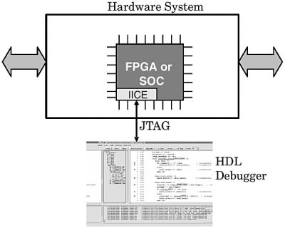
Figure 18-1 shows a block diagram of how this works. The VHDL for the device is read into a tool that automatically creates and inserts a small debug core into the device that probes internal signals. The debug core is created based on information from the designer about what signals are to be probed. This debug core communicates through the JTAG port on the device to an HDL debugger executing on a host platform. The HDL debugger sends and receives data from the debug core and displays this data in context with the HDL for the design. Waveforms of the internal device data can also be displayed, providing the ability to trace down problems in the design.
This technique works well for any design, but it works especially well for designs where a tremendous amount of data must be processed by the...