Designing with FPGAs and CPLDs
In this easy to follow guide, the author provides a look at the proprietary designs and methods of CPLDs and FPGAs available to managers, designers and engineers.
Field Programmable Gate Arrays are given this name because they are structured very much like a gate array ASIC. Like an ASIC, the FPGA consists of a regular array of logic, an architecture that lends itself to very complex designs.
This chapter describes the architecture and technologies of FPGAs. This chapter should help you:
Understand the internal architecture of FPGAs
Gain knowledge of the technologies used for programming and connecting internal blocks of FPGAs
Learn the advantages and trade-offs of different architectures and technologies
Learn the differences between CPLDs and FPGAs
Each FPGA vendor has its own FPGA architecture, but in general terms they are all a variation of that shown in Figure 3.1. The architecture consists of configurable logic blocks, configurable I/O blocks, and programmable interconnect to route signals between the logic blocks and I/O blocks. Also, there is clock circuitry for driving the clock signals to each flip-flop in each logic block. Additional logic resources such as ALUs, memory, and decoders may also be available. The two most common types of programmable elements for an FPGA are static RAM and antifuses. Antifuse technology is a cousin to the programmable fuses in EPROMs. You will learn about antifuses, along with these other aspects of FPGAs, in the following sections.
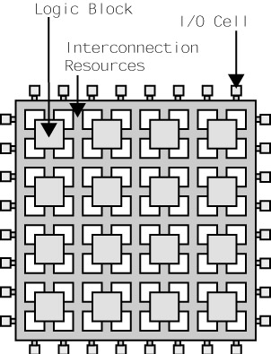
The important thing to note about the FPGA architecture is its regular, ASIC-like structure. This regular structure makes FPGAs useful for all kinds of logic designs.