Designing with FPGAs and CPLDs
In this easy to follow guide, the author provides a look at the proprietary designs and methods of CPLDs and FPGAs available to managers, designers and engineers.
Top-down design is the design methodology whereby high level functions are defined first, and the lower level implementation details are filled in later. A design can be viewed as a hierarchical tree, as shown in Figure 5.1. The top level block represents the entire chip. The next lower level blocks also represent the entire chip but divided into the major function blocks of the chip. Intermediate level blocks divide the functionality into more manageable pieces. The bottom level contains only gates and macrofunctions, which are vendor-supplied high level functions.
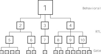
Top-down design methodology lends itself particularly well to using HDLs, the generally accepted method of designing complex CPLDs and FPGAs. Each block in the design corresponds to the code for a self-contained module. The top-level blocks correspond to the behavioral models that comprise the chip. The intermediate levels correspond to the RTL models that will become input to the synthesis process. The lowest level of the hierarchy corresponds to gate level code which is output from the synthesis software and which directly represents logic structures within the chip.
Top-down design methodology works hand in hand with a written specification that, as discussed in Chapter 4, is an essential starting point for any design. The specification must include general aspects of the design, including the major functional blocks. The highest blocks of a top-down design are behavioral level models that correspond to the major...