Electronic Devices and Amplifier Circuits with MATLAB Computing, Second Edition
Emphasizing operational amplifiers and integrated devices used in digital circuits, this text presents a thorough discussion of state-of-the-art electronic devices.
In our previous discussion, for convenience, a separate voltage source V BE has been used to provide the necessary forward-bias voltage and another voltage source V CC to establish a suitable collector voltage V C where V C=V CC R CIC. However, it is not practical to use a separate emitter-base bias voltage V BE. This is because conventional batteries are not available for 0.7 V. For this reason we use resistors in the order of kilohms to form voltage dividers with desired values. In addition to eliminating the battery, some of these biasing methods compensate for slight variations in transistor characteristics and changes in transistor conduction resulting from temperature irregularities.
Figure 3.21 shows the basic NPN transistor amplifier where resistor R B provides the necessary forward bias for the emitter-base junction. Conventional current flows from V CC through R B to the base then to the grounded emitter. Since the current in the base circuit is very small (a few hundred microamperes) and the forward resistance of the transistor is low, only a few tenths of a volt of positive bias will be felt on the base of the transistor. However, this is enough voltage on the base, along with ground on the emitter and the large positive voltage on the collector to properly bias the transistor.
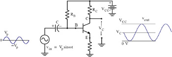
With the transistor properly biased, direct...