Electronic Devices and Amplifier Circuits with MATLAB Computing, Second Edition
Emphasizing operational amplifiers and integrated devices used in digital circuits, this text presents a thorough discussion of state-of-the-art electronic devices.
 TABLE OF CONTENTS
 The circuit shown in Figure 3.50 is a model to represent the transistor where the two ideal diodes are included to remind us of the two PN junctions in the transistor.
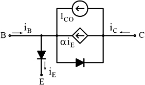
In Figure 3.50, I CO is the current into the reverse-biased collector with i E = 0. By KCL,

and since i E=i C+i B
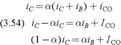
or

From Table 3.1

Also,
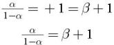
and by substitution into (3.55)

Thus, the equivalent circuit in Figure 3.50 may be redrawn as shown in Figure 3.51.
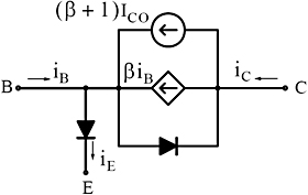
The transistor models shown in Figures 3.50 and 3.51 are essentially ideal models. An improved transistor model is shown in Figure 3.52 where for silicon type of transistors V D ?0.7 V and r b, referred to as the base spreading resistance, is included to account for the small voltage drop in the base of the transistor.
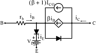
Analogous to the base resistance r b are the emitter diffusion resistance defined as

and the collector resistance

Typical values for r b are between 50 ? to 250 ?, for r e are between 10 ? to 25 ?, and r c is very high, in excess of 1 M ?. The model in Figure 3.52 is for an NPN transistors. It applies also to PNP transistors...