Fundamentals of Microsystems Packaging

Dr. Phil Garrou Dow Chemical
Prof. Rao R. Tummala Georgia Institute of Technology

Explain the reasons for wafer-level packaging
Compare and contrast wafer-level packaging with other packaging technologies
Describe various wafer-level technologies under development and in use
Describe wafer-level burn-in and test methodologies
Project the future of wafer-level packaging
The recent trend to portable and wireless on one hand, and commodity prices for cell phones and PCs on the other hand, has brought on the need for much smaller IC and system-level packages that are also low in cost. Wafer-level packaging, described in this chapter, addresses these needs at the IC packaging level.
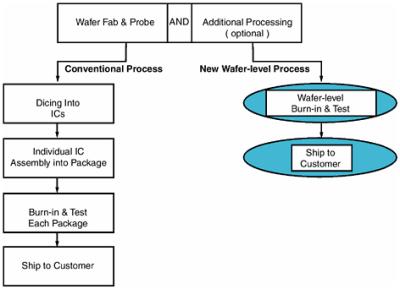
Wafer-level packaging (WLP) is IC packaging formed at the wafer level on the wafer in the wafer foundry. This is in contrast to conventional packaging that is done in two parts wafer and singulation of that wafer into ICs and the subsequent packaging of these ICs into QFP, BGA, CSP or other packages. In this new process, front-end IC fabrication and back-end IC assembly are performed at the wafer foundry. The basic concept is to take the wafer immediately after fabrication but before test, and form IC connections with a few more process steps with which to test and burn-in before singulating into packaged ICs. Figure 10.1 illustrates the basic differences between today s wafer and IC packaging vs. the new wafer level packaging process.