Fundamentals of Microsystems Packaging

Mahesh Varadarajan Indian Institute of Science, India
Prof. Zsolt Illyefalvi-Vite z UTE, Budapest
Dr. Joachim Zimmermann Bosch, Germany
Prof. Rao R. Tummala Georgia Institute of Technology

Define printed wiring board (PWB) and describe its functions.
Given the anatomy of a PWB, introduce and define all the critical elements of a PWB.
Introduce and describe the CAD tools for PWB design.
Describe standard materials and processes typically used in fabricating PWBs.
Describe the limitations of PWBs and describe how microvia solves the problem.
Describe various microvia technologies recently developed.
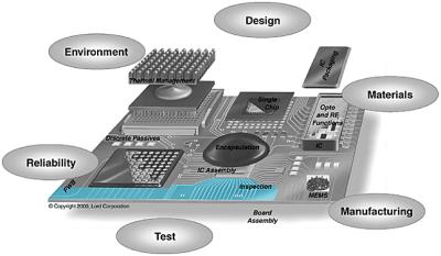
Printed wiring boards allow both active and passive components to be interconnected, powered, cooled and protected to form electronic systems. This chapter describes the materials, processes, and designs, both for conventional laminated printed wiring boards and for advanced microvia-based boards.
A printed wiring board (PWB), or printed circuit board (PCB), is a composite of organic and inorganic materials with external and internal wiring, allowing electronic components to be electrically interconnected and mechanically supported. In addition, a PWB must provide power to the components and conduct away heat when necessary. The boards are also called motherboards or system-level boards, because they carry all of the components required for that system or subsystem. They are also called back planes when some of the boards are interconnected to a larger motherboard.
Every electronic system contains at least one PWB, some of which are electrically interconnected...