Integrated Circuit Packaging, Assembly and Interconnections
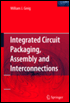
Chapter 4: The Chip Scale Package

4 THE CHIP SCALE PACKAGE, CSP

The Chip Scale Package introduced in the early 90s is essentially a smaller version of the BGA and represents the continuing trend in package miniaturization.

Industry arbitrarily defines a CSP as any package that is no larger than 1.2 times the area of the die. However, in many instances a package is classified as a CSP if it is simply near-die size . CSPs share many of the same attributes as the flip chip including areas of application.

When first introduced, the CSP was presented as a viable alternative to the flip chip, particularly in size, but offering all the advantages of a packaged device including pre-assembly testing and easier handling. An important feature of the CSP that differentiates it from the flip chip is that both the bumps and bump pitch are larger (>0.2 mm, 8 mils) than those of the flip chip (typically 4 5 mils). Figure 4-1 illustrates how the BGA and the CSP compare relative to package size and bump diameters.


Figure 4-1: BGA vs. CSP

This is a significant attribute since it can enhance reliability and requires a less sophisticated and more readily available PWB. While the flip chip is applicable to the full spectrum of I/O count the CSP is more appropriate to the lower end.

The number of package pads that can be accommodated will typically depend upon the bump size and pitch, and overall die size.

The larger the bump and the bump pitch the less I/Os...

UNLIMITED FREE ACCESS TO THE WORLD'S BEST IDEAS

SUBMIT
Already a GlobalSpec user? Log in.

This is embarrasing...

An error occurred while processing the form. Please try again in a few minutes.

Customize Your GlobalSpec Experience

Category: Battery Charger ICs
Finish!
Privacy Policy

This is embarrasing...

An error occurred while processing the form. Please try again in a few minutes.