Electro-Optics Handbook, Second Edition
Developed by a towering figure in the field, this valuable, all-inclusive guide thoroughly explains and discusses the use of optical devices and light in electronics systems.
Martin Peckerar, P.-T. Ho, and Y. J. Chen
For many years, miniature light sources such as light-emitting diodes (LEDs) and solid-state lasers have been combined with diode sensors through a variety of optical channels and modulators on a single integrated substrate.1 Prismatic couplers allowed off-chip communication.2 Standard integrated circuit patterning technology (optical lithography and wet chemical etching) was used to make these structures. Although demands on resolution and process robustness were not great in the past, new generations of optoelectronic devices place strin-gent demand on patterning technology.
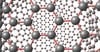
Semiconductor layered structures can be fabricated with predetermined band-gaps through the emerging field of bandgap engineering.3 ,4 Artificial superlattices created by multilayer epitaxy enable the fabrication of laser sources and sensors tuned to a wide range of optical wavelengths. To improve laser efficiency, grating structures and confining cavities are created as integral parts of these devices. Minimum feature sizes of these gratings are on the order of the wavelength of light propagating through the device.
State-of-the-art devices may even make use of quantum mechanical phenomena to achieve low threshold currents and narrow tunable linewidths, etc. Such quantum-effect (QE) devices are possible as a result of the ability to create materials structures whose critical dimensions are on the order of the diameter of an electron-wave packet in the transport medium. Initially, QE device fabrication was accomplished by using the precise thickness control possible in thin-film layered deposition. This vertical thickness control, combined with the ultraclean crystal-growing capability of molecular beam epitaxy...