Low Power Methodology Manual: For System-on-Chip Design
Taking a practical approach, rather than a theoretical approach, this book describes a number of the techniques designers can use to reduce the power consumption of complex SoC designs.
This chapter describes power gating design from a front-end, RTL perspective. Figure 5-1 shows the critical components of such a design.
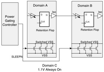
The critical issues in power gating include the design of the switching network and the power gating controller. We also need to determine when and where to insert retention flops and isolation cells.
The detailed transistor structures for power gating are highly technology specific and are described in detail in Appendix A. But we will consider here some of the architectural aspects of the switching fabric design.
The first architectural issue is whether to switch VDD (with a "header" switch) or to switch VSS (with a "footer" switch) or both.
A number of academic papers have been published on this subject. Some authors advocate both P-channel "Header" switches gating the VDD supply and N-channel "Footer" switches gating the VSS ground. However, two such high-V T power switches in series with the gate cause a more significant IR voltage drop in the supply as seen by the gate. This drop in turn causes increased delays for the gates in the design.
In many practical designs this performance loss cannot be tolerated, and only one of the rails is switched.
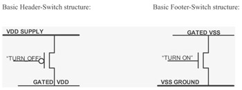
With a header-style switch fabric, the internal nodes and outputs of a power gated block collapse down towards the ground rail when the switch is turned off. With a footer-style switch fabric the internal nodes and outputs all charge...