Low Power Methodology Manual: For System-on-Chip Design
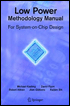
Taking a practical approach, rather than a theoretical approach, this book describes a number of the techniques designers can use to reduce the power consumption of complex SoC designs.
 TABLE OF CONTENTS
 The previous chapter introduced Dynamic Voltage Scaling and Adaptive Voltage Scaling. This chapter describes two examples of voltage scaling: the ULTRA926 and the ATLAS926. Both chips were designed as technology demonstrators for low power design techniques.
The ULTRA926 technology demonstrator chip used an ARM926EJ-S as a test vehicle for Adaptive Voltage Scaling. The ULTRA926 was a collaborative effort between ARM, Synopsys, Artisan, NSC, and UMC. The overall SoC design was developed by ARM for UMC with Synopsys providing the EDA methodology and implementation, Artisan providing the IEM-specific cell library and PLL components, and National Semiconductor Corporation providing Adaptive DVFS (AVS) power supply technology.
The chip was implemented using UMC's 130nm process. This process has a nominal supply rail voltage of 1.2V, which leaves some useful headroom to apply DVFS techniques and obtain valuable energy savings.
As a methodology development vehicle this presents the primary design and verification problems that have to be addressed for full-scale product designs.
As shown in Figure 10-1 the ULTRA926 system supports both DVFS and AVS.
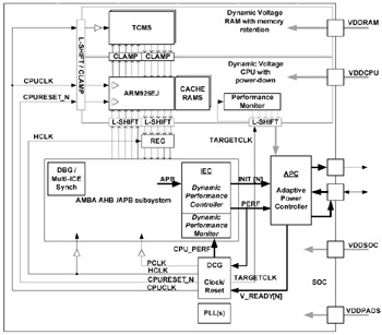
The cache memories and CPU standard cell logic share the VDDCPU power domain as there was sufficient headroom to voltage scale the memories in this technology. So they are voltage scaled and power gated together.
The tightly coupled memories (TCMs) have their own voltage-scaled domain, VDDRAM, which is scaled with the VDDCPU voltage in functional use, but can also be kept...