Low Power Methodology Manual: For System-on-Chip Design
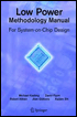
Taking a practical approach, rather than a theoretical approach, this book describes a number of the techniques designers can use to reduce the power consumption of complex SoC designs.
 TABLE OF CONTENTS
 Scaling the supply voltage of CMOS is possible over a technology-specific range; gate delays, setup and hold times and even memory access times scale monotonically with reduced operating voltage over a limited range. Linear voltage reduction results in a square-law reduction in both dynamic power consumption and in leakage power.
The earlier chapters have focused on basic multi-voltage techniques for optimizing dynamic power and on techniques to address leakage on advanced technology nodes. Voltage Scaling reducing the supply voltage and clock frequency based on work load is a more aggressive technique for dynamic power reduction. It can be effective on 0.18u and 0.13u technology nodes (typically 1.8 and 1.2V standard operating voltage respectively) where there is significant voltage headroom. In generic 90nm nodes (and below) there is not sufficient headroom to use voltage scaling very effectively. But it can be applicable to the "Low-Leakage" technology nodes at 90nm, 65nm and below, since these run at higher voltage than the equivalent generic or high-speed processes. (The 90nm low voltage processes run at 1.2V nominal voltage compared to 1.0V for the "generic" or high-speed process nodes, for example).
Voltage scaling introduces complications into both the system design and the implementation flow, but can be valuable for portable battery-powered products. Rarely is all the logic on a SOC required to run at the limit of performance at all times, and in many systems there may be several different performance profiles. Dynamically scaling the supply voltage to a processor or multi-media...