Low Power Methodology Manual: For System-on-Chip Design
Taking a practical approach, rather than a theoretical approach, this book describes a number of the techniques designers can use to reduce the power consumption of complex SoC designs.
Partitioning a design into separate power domains introduces new interfaces between each power domain. These added interfaces may contain isolation cells and level shifters. Thus, the specific partitioning can have a significant impact on the overall performance of the design.
The job of partitioning a design into power domains is a joint responsibility of the system architect(s), RTL designer(s), and implementation engineer(s). Between them they understand the target application, the power and performance objectives, and the limitations of the target technology.
When mapping the logical hierarchy to power domains, we want to assign hierarchical functional units in their entirety wherever possible. Synthesis engines operate top down on a cell in the hierarchy and the best Quality of Results (QoR) is achieved if the entire hierarchy can be manipulated under the same goals and constraints.
Gathering up various hierarchical cells from different levels of the design and assigning them to power domains can make timing closure significantly more difficult.
Figure 11-3 shows the logical hierarchy of the ARM1176JZF-S after some logical grouping of top level modules in preparation for a low power implementation.
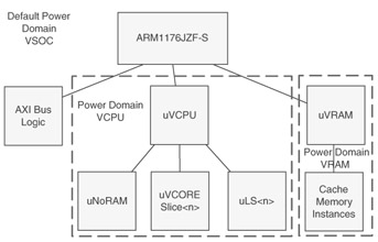
In this example, we map the entire CPU to the VCPU domain, the whole cache logic and RAMS to the VRAM power domain, and the AXI bus to the VSOC power domain.
This partitioning meets several objectives:
In some power modes, we power gate the CPU, but keep the...