Low Power Methodology Manual: For System-on-Chip Design
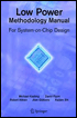
Taking a practical approach, rather than a theoretical approach, this book describes a number of the techniques designers can use to reduce the power consumption of complex SoC designs.
 TABLE OF CONTENTS
 Power gating is the most effective method for reducing leakage power in standby or sleep mode. However, this method comes with overhead such as the silicon area taken by the sleep transistors, the routing resources for permanent and virtual power networks, and the complex power-gating design and implementation processes which impact design risk and schedule.
Besides the overhead, power gating introduces power integrity issues such as IR drop on the sleep transistors and ground bounce caused by in-rush wakeup current. It also introduces wakeup latency, the time needed to restore full power for normal operation. All these issues must be addressed during the implementation of power gating designs.
In this chapter, we discuss:
power gating implementation styles
wakeup in-rush current control
wakeup and sleep latency reduction
sleep transistor power network synthesis
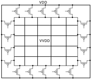
Coarse grain power gating can be implemented in either a ring or a grid style power network.
With ring based switching, we place the switches externally to the power gated block effectively encapsulating the block with a ring of switches.
In the grid style implementation, the sleep transistors are distributed throughout the power gated region.
Figure 14-1 shows an example of a ring implementation. A ring of VDD surrounds the power gated block. A ring of switches connects VDD to a switched or virtual VDD (VVDD) power mesh that covers the power gated block.
Note that a ring style switching network is...