Low Power Methodology Manual: For System-on-Chip Design
Taking a practical approach, rather than a theoretical approach, this book describes a number of the techniques designers can use to reduce the power consumption of complex SoC designs.
As show in Figure 11-4, the design flow for a multi-voltage, power gating design follows that of a standard implementation with a few exceptions.
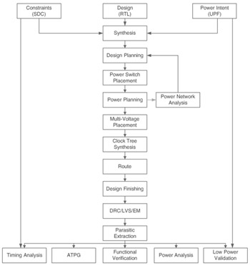
Primarily, the differences between the standard design flow and that for a multi-voltage, power gated design are:
Specification of the power intent
Creation of power domains during synthesis
State retention synthesis with always-on network management
Multi-voltage physical design partitioning and the addition of MTCMOS switch cells
Multi-voltage power network synthesis for MTCMOS power gating during power planning phase
Early power network analysis to validate power gating switch topology
Multi-voltage placement optimization including level shifter and isolation cell optimization
Multi-voltage clock tree synthesis and optimization
Intensive post route power network analysis with power-up sequencing verification