Electronic Instrument Handbook, Third Edition
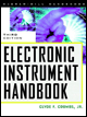
The material used in the manufacture of Hall-effect devices is a p-type or an n-type semiconductor. Typical examples are indium arsenide, indium arsenide phosphide, and doped silicon. Figure 5.15 shows a section of a p-doped semiconductor subjected to a magnetic field B z in the z direction and an electric field E x in the x direction. A current I x flows in the x direction.
The holes move in the x direction across the magnetic field and experience an upward magnetic force, which results in the accumulation of holes on the top surface and electrons on the bottom face, as indicated in Fig. 5.15. An electric field E y , known as the Hall field, is set up as a consequence, and this is known as the Hall effect.31 The corresponding Hall voltage V H= E y t. Since there is no flow of current in the y direction, the magnetic force equilibrates with the electric force that is exerted on the holes, and as a result the Hall voltage can be expressed as
| (5.17) | |
where R H is the Hall coefficient. R H is negative for an n-type semiconductor. h is the dimension parallel in B z . Equation...