Digital Electronics and Design with VHDL

Chapter 20: VHDL Design of Combinational Logic Circuits

Overview

Objective: Combinational circuits were studied in Chapters 11 and 12, with logic circuits in the former and arithmetic circuits in the latter. The same division is made in the VHDL examples, with combinational logic designs presented in this chapter and Combinational alarithmetic designs illustrated in the next.

Chapter Contents

20.1

Generic Address Decoder

20.2

BCD-to-SSD Conversion Function

20.3

Generic Multiplexer

20.4

Generic Priority Encoder

20.5

Design of ROM Memory

20.6

Design of Synchronous RAM Memories

20.7

Exercises

20.1 Generic Address Decoder

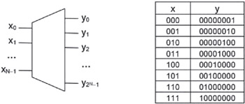
Address decoders were studied in Section 11.5. We illustrate now the design of the address decoder of Figure 20.1 (borrowed from Figure 11.7) in the following two situations:

  • With N = 3 using the WHEN statement (for N = 3, the truth table is shown in Figure 20.1).


    Figure 20.1: Address decoder. The truth table is for the case of N = 3

  • Still using WHEN, but for arbitrary size (generic N).

Code for N = 3 using the WHEN Statement

A VHDL code for this problem is shown below. As mentioned in Section 19.2, three sections of code are necessary. However, the first (library declarations) was omitted because only the standard libraries are employed in this example, and these are made visible automatically.

The second section of code ( ENTITY) is responsible for defining the circuit's I/O ports (pins) and appears in lines 2 5 under the name address_decoder; it declares x

UNLIMITED FREE
ACCESS
TO THE WORLD'S BEST IDEAS

SUBMIT
Already a GlobalSpec user? Log in.

This is embarrasing...

An error occurred while processing the form. Please try again in a few minutes.

Customize Your GlobalSpec Experience

Category: Logic Encoders
Finish!
Privacy Policy

This is embarrasing...

An error occurred while processing the form. Please try again in a few minutes.