Diodes Information
A semiconductor diode is a non-linear device whose most outstanding feature is the fact that, basically, current is only allowed to flow in one direction. The diode is built by joining together two semiconductor materials: an N-type material (rich in negative carriers or free electrons) and a P-type material (rich in positive carriers or holes). The area of contact is called the junction. For this reason the diode is commonly referred to as a PN Junction.
When an applied voltage forces the diode to conduct electrons from the anode to the cathode it is operating in a forward bias condition. When the applied potential does not allow for a sharp increase in current and only a minimal amount, practically zero, of current is observed across the junction, the diode is said to be in a reverse bias condition. When forward biased the diode behaves much like a closed switch, and when reverse biased the diode behaves like an open switch.
The following schematic symbol is used to represent a diode:
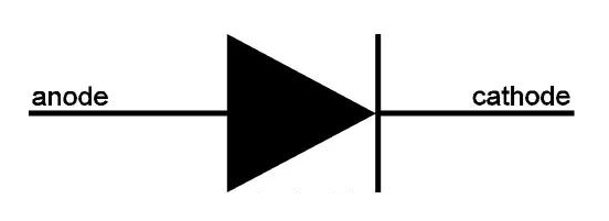
Image Credit: GotToKnow.com
The anode represents the P-type material and the cathode is the N-type material of the junction.
Diode Operation
The operation of a diode is controlled by the diode's current-voltage (I-V) characteristics. A diode in a circuit with the positive potential (highest) connected to the P material and the negative potential connected to the N material is forward biased. A diode whose highest potential is connected to the N material and the lowest potential to the P material is reverse biased.
The following figure shows the forward and reversed biasing of a diode connected to a circuit.
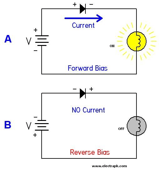
Image Credit: Electrapk
Diode Characteristics
The typical I-V characteristics of a diode are illustrated by the following figure. There are two operating regions that are clearly labeled: the forward bias region and the reverse bias region. Two scales are used along each axis to depict the varied response of the diode both in the positive and negative directions. A forward biased current in this particular I-V curve is expressed in milli-amps (mA), whereas in the reverse bias region the current is expressed in micro-amps (μA). The main features of these two operating conditions are explained below.
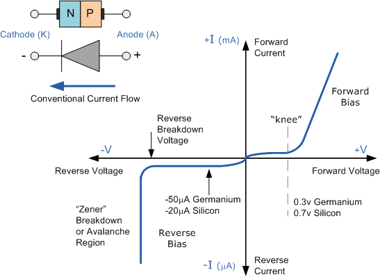
Image Credit: Nikhil.M.R
Forward Bias Region
In the forward bias region there exist two important areas to distinguish in relation to the amount of current observed through the diode. The first area is when there are low levels of diode voltage (VD) and the associated current is very small. The second area is when the diode voltage (VD) is greater than the threshold voltage (Vthr), and the current increases abruptly.
Diode Voltage is < Vthr - For any diode voltage (VD) between zero and (Vthr) the current is very small. In general, as an approximation, we may consider this current to be zero. This means that in this range the diode behaves like an open switch, or like a device with a very high resistance.
Diode Voltage is ≥ Vthr - For any diode voltage (VD) greater than (Vthr) the current increases abruptly. In general, as an approximation, we may consider the resistance to be zero. This means that in this range the diode behaves like a closed switch.
The response to an applied voltage in the forward bias region is controlled by the diode's threshold voltage, which is dependent on the type of material the diode is built with. A silicon diode has an approximate value of Vthr = 0.7 V, and a germanium diode has an approximate value of Vthr = 0.3 V.
Reverse Bias Region
In the reverse bias region there also exists two important areas that can be distinguished in relation to the amount of the current observed through the diode. The current through the diode is very small, practically zero, when the diode voltage is between zero and the breakdown voltage (VBD). Beyond the breakdown voltage (VBD) there is an abrupt increase in current, which marks the second area of interest in the reverse bias region.
Diode Voltage is < VBD - In this area the current is very small. We call this current the leakage current. In practical applications you may consider it to be zero. Thus, in this area the diode behaves like an open switch, or like a device with a very large resistance.
Diode Voltage is ≥VBD - In the breakdown region the current increases very fast as a function of the diode voltage. The diode behaves like a closed switch, or like a device with a very small resistance. Notice that the diode voltage in this case is very close to VBD for practical applications, for any source voltage.
The breakdown voltage is not a constant value like the threshold voltage in forward bias. VBD is different for each diode. This value is a specification parameter given by the manufacturer.
The following table is a summary of the diode operating conditions. The last column of the table indicates the behavior of an ideal diode. When an ideal diode is forward biased it would behave like a closed switch with a resistance equal to zero ( 0 W ). In reverse bias the ideal diode is similar to an open switch with current equal to zero and infinite ( ∞ Ω ) resistance.
|
Diode Voltage (VD) |
Current |
Resistance |
Ideal Behavior |
| Forward Bias |
≈ 0 |
very large |
open switch |
| (VD < Vthr) |
( ≈ ∞ ) |
||
| Forward Bias |
large |
very small |
closed switch |
| (VD ≥ Vthr) | |||
| Reverse Bias |
≈ 0 |
very large |
open switch |
| (VD < VBD) |
( ≈ ∞ ) |
||
| Reverse Bias |
large |
very small |
closed switch |
| (VD ≥ VBD) | |||
Diode Identification
The schematic symbol used for the diode is typically an arrow with a short line across the tip. The cathode is the N-type material and is represented by the tip of the arrow. The anode is the P-type material and is indicated by the base of the arrow.
Manufacturers may use diverse methods to indicate the anode and the cathode of the diode. In the most common method the cathode (N-type material) is identified with a colored band. Thus, the end of the diode closest to this band is the cathode. The other end is the anode (P-type material.)
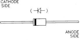
Image Credit: Integrated Publishing
Diode Specifications
The important specifications of diodes depend on the type of diode and its applications. In what follows we list the most important specifications for all types of diodes.
-
Forward voltage (VF) is the voltage across the diode terminals resulting in a sharp increase of current in the forward direction.
-
Forward current (IF) is the current when the forward voltage is applied; it flows through the diode in the direction of lower resistance.
-
Reverse current (IR) or leakage current, is the current value when the reverse voltage is applied. This is the current that flows when reverse bias is applied to a semiconductor junction.
-
Reverse voltage (VR) is the maximum allowable reverse voltage that can be applied repeatedly.
-
Breakdown voltage (VBR) is the reverse voltage at which a small increase in voltage results in a sharp rise of reverse current.
-
Power Dissipation (PD) is the maximum permissible power dissipation per output (in W) of the diode at specified ambient temperature. Power dissipation is the power dissipated by the diode while in the ON state.
-
Junction operating temperature (Tj) is the range of temperatures at which a diode is designed to operate.
Types of Diodes
The term diode can be used to describe a typical PN diode, also known as a general purpose diode, or it may be used as a broader term to describe one of many other types of diodes. A specific type of diode may be used for a particular application or exhibit a specific behavior or characteristic. The following descriptions and illustrations cover a short list of common and special purpose diodes.
General purpose diodes are two-terminal electronic components that allow current to flow in only one direction, from an anode (+) to a cathode. These simple semiconductors are PN junctions with a positive or P-region with positive ions and a negative or N-region with negative electrons. Applying a forward voltage to the PN junction causes current to flow in only one direction as electrons from the N-region fill "holes" in the P-region. The diode's reverse voltage is the potential barrier that prevents current to flow in the opposite direction, analogous to a pressure rating on a check valve.

Image Credit: AMB Laboratories
Light emitting diodes (LEDs) are PN junction devices that give off light radiation through electroluminescence when forward biased. They are used as various indicators in aviation, automotive and traffic lighting, as well as lighting for some lamps and torches. Most light emitting diodes function in the near infrared and visible ranges, though there are now UV LEDs as well.
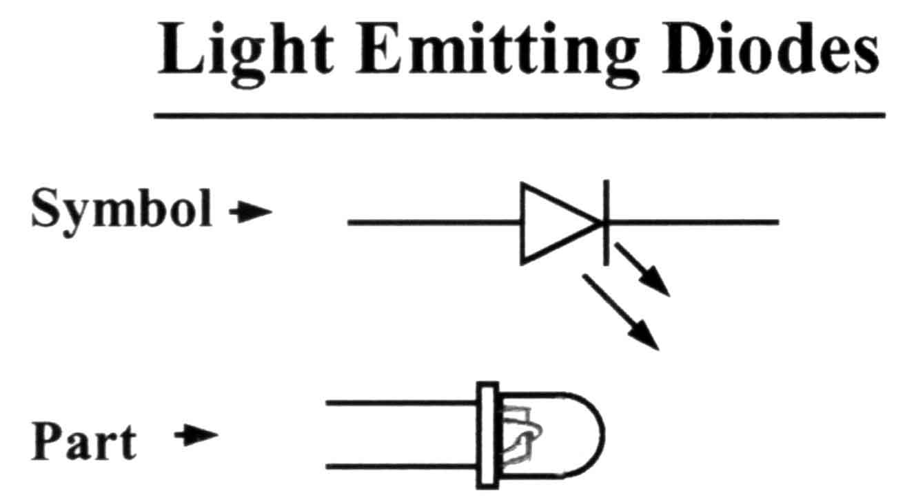
Image Credit: MRISAR
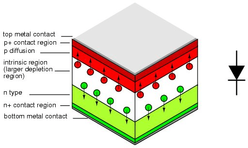
Photodiodes are a two electrode, radiation sensitive junction formed in a semiconductor material in which the reverse current varies with illumination. Photodiodes are used for the detection of optical power and for the conversion of optical power to electrical power. Photodiodes can be PN, PIN, or avalanche. PN photodiodes feature a two electrode, radiation sensitive PN junction formed in a semiconductor material in which the reverse current varies with illumination. PIN photodiodes are diodes with a large intrinsic region sandwiched between P-doped and N-doped semiconducting regions. Photons absorbed in this region create electron-hole pairs that are then separated by an electric field, thus generating an electric current in a load circuit. Avalanche photodiodes are devices that utilize avalanche multiplication of photocurrent by means of hole-electrons created by absorbed photons. When the device's reverse-bias voltage nears breakdown level, the hole-electron pairs collide with ions to create additional hole-electron pairs, thus achieving a signal gain.

Image Credit: MCU Tutor
PIN diodes are three-layer semiconductor diodes consisting of an intrinsic layer separating heavily doped P and N layers. The charge stored in the intrinsic layer in conjunction with other diode parameters determines the resistance of the diode at RF and microwave frequencies. This resistance typically ranges from kilohms to less than 1 ohm for a given diode. PIN diodes are typically used as switches or attenuator elements.
Image Credit: All About Circuits
Rectifiers receive an alternating current (AC) with an average value of zero volts and supply a direct current (DC), single polarity signal with a net value greater than zero volts, a process otherwise known as rectification. The essential component in a rectifier is the diode. The diode is an electronic component that allows current to flow in only one direction, from an anode (+) to a cathode (-). A single rectifier diode will only allow half of an AC signal to propagate while blocking the reverse polarity so long as it does not exceed the breakdown voltage. Several circuits are available that allow for half-wave and full-wave rectification.
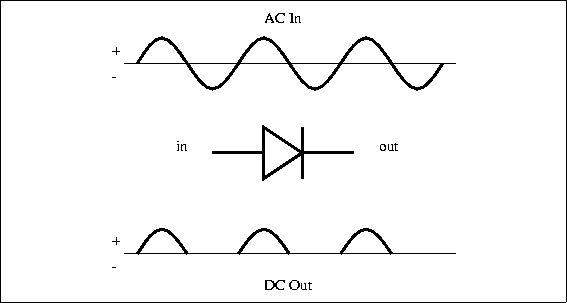
Image Credit: Marine Insight
Schottky diodes are also known as Schottky barrier diodes or hot-carrier diodes. They consist of a junction between a metal layer and a semiconductor element. The metal layer, a cathode, is heavily occupied with conduction-band electrons. The semiconductor element, an anode, is a lightly doped N-type semiconductor. When forward-biased the higher energy electrons in the N region are injected into the metal region allowing the junction to operate in the ON state. Schottky diodes achieve high switching speeds as they give up their excess energy very rapidly as they fluctuate between ON and OFF states.

Image Credit: Electrical-Info.com
Tunnel diodes are heavily doped P-N diodes in which electron tunneling from the conduction band in the N-type material to the valence band in the P-type region produces a region of negative resistance. This negative-resistance region is the most important area of operation. As the voltage is increased, the current decreases. This feature makes tunneling diodes especially useful in low power oscillators and radio frequency (RF) applications.
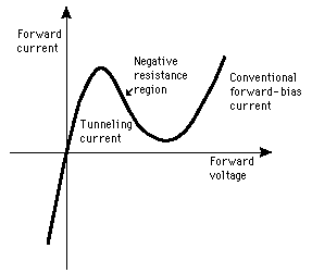
Image Credit: HyperPhysics
Varactor diodes are p-n junction diodes that are designed to act as a voltage-controlled capacitor when operated under reverse bias. When a PN junction is biased by applying a voltage to the junction, it results in a negative charge on the P side and positive charge on the N side. The region between these positive and negative charges, known as the depletion region, does not contain any moving charges.
The inherent capacitance is the resultant from the biased junction: two opposing charges separated by an insulator. In fact, all PN junctions have an associated capacitance (Cj) and when voltage is applied to the diode, the depletion region decreases (forward bias) or increases (reverse bias), changing the value of the PN junction capacitance.
Varactors are manufactured so that the PN junction capacitance has a known and controllable relation to the applied diode voltage. This voltage-controlled capacitance is normally produced strictly using a reverse bias only. The following figure shows the layout, the symbol and the curve that shows the relationship between the applied reverse bias voltage and the capacitance.

Image Credit: Polytech Lille
Note that as the reverse bias voltage (VR) increases the capacitance decreases. The quality CT is the capacitance of the device when there is no applied voltage. The relation between the reverse bias voltage and the capacitance is given by the following formula:
![]()
Where:
Cj = Junction Capacitance
CT = Terminal Capacitance
VR = Reverse Bias Voltage
Zener diodes are PN junction devices that are designed to operate in the reverse-breakdown region. The breakdown voltage (Vz) of Zener diodes is set by carefully controlling the doping level during manufacture. This breakdown phenomenon is referred to as the Zener voltage or the Zener effect.

Image Credit: TDK Lambda UK
|
Diode Type |
Characteristics |
Application |
|
Light Emitting Diode (LED) |
PN Junction Device that Emits Light Radiation |
Illumination / Optical Signal Transmitter |
|
PN Junction Diode |
Conduct Current from an Anode (+) to a Cathode (-) |
General Purpose |
|
Photodiode |
Opto-electronic Device in which the Reverse Current Varies with Illumination |
Detection / Conversion of Optical Power |
|
PIN Diode |
Increased Depletion Area; Lower Capacitance; Higher Reverse Breakdown Voltage |
High Voltage Rectification, RF Switch; Photodetector |
|
Rectifier |
Conducts a Direct Current (DC), Single Polarity Signal with a Net Value Greater than Zero Volts |
Rectification |
|
Schottky Diode |
Low Forward Voltage; No Reverse Recovery Time |
High Frequency; High Speed Switching |
|
Tunnel Diode |
Region of Negative Resistance in Forward Bias Region; Narrow Depletion Region |
Low Power Gain; High Frequency; High Speed Switching |
|
Varactor Diode |
Capacitance is a Function of Reverse Bias Voltage; Used as a Variable Capacitor |
VCO; RF Filters |
|
Zener Diode |
Conducts Current when Reverse Bias reaches VBR; Constant Output Voltage; Sharp Increase In Current @ VBR |
Power Supplies; Voltage Regulation |
Product Lifecycle Stages
Diodes follow product lifecycle stages that are defined by the Electronic Industries Alliance (EIA) in EIA-724. The six distinct phases of a product's life cycle recognized by EIA-724 are: Introduction, Growth, Maturity, Saturation, Decline, and Phase Out.
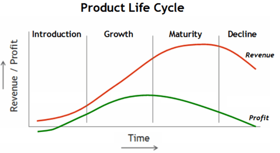
Image Credit: UIUC
-
Introduction - Product planning or design is underway. Samples may or may not exist. Specification changes may occur and planned introduction dates may be delayed. Orders and product shipments are not permitted.
-
Growth - Production is increasing rapidly. Manufacturing capacity is being added. Orders and shipments are permitted.
-
Maturity - Product growth has stabilized or peaked. Product quality is very high. Orders and shipments are permitted. Product is recommended for use in new designs.
-
Saturation - Sales and capacity have peaked. Orders and shipments are permitted.
-
Decline - Capacity is beginning to decline. Orders and shipments are permitted, but devices are not recommended for new designs
-
Phase Out - Capacity is declining rapidly. A formal discontinuance notice may be issued. Limitations on shipments can occur, but orders are still allowed. Devices are not considered for new designs.
RoHS Compliance
Image Credit: Industrial Safety Solutions
Restriction of Hazardous Substances (RoHS) is a European Union (EU) directive that requires all manufacturers of electronic and electrical equipment sold in Europe to demonstrate that their products contain only minimal levels of the following hazardous substances: lead, mercury, cadmium, hexavalent chromium, polybrominated biphenyl and polybrominated diphenyl ether. RoHS became effective on July 1, 2006.
Resources
- Avalanche Diodes
- Current Limiting Diodes
- Detector
- General Purpose (PN Junction Diodes)
- High Voltage
- Limiter
- Low Leakage
- Mixer
- Modulation
- PIN Diodes
- Power Diode
- Protector
- RF Diodes
- Rectifier Diode
- RoHS Compliant
- Schottky Barrier Diodes
- Step-recovery Diodes
- Switching
- Transient Voltage Suppressor Diodes (TVS)
- Tunnel Diodes
- Varactor Diodes
- Voltage Regulation
- Zener Diodes
- microwave diode
- 3 phase bridge rectifier
- avalanche diode
- list of germanium diode
- 200 amp diodes
- 940nm laser diode
- diode laser bar
- diode SMD
- high frequency diodes
- temperature sensitive diode
- thermal diode
- types of diodes and their application
- 440 nm diode laser
- 470nm laser diode
- 808nm laser diode
- 915nm laser diode
- alignment laser diode
- axial leaded diode
- Bi-Directional diode
- diode network
- diode rectifier 10 GHz
- diode varactor simulation
- diodes for welder
- ESD protection diode
- external cavity diode laser
- fiber coupled laser diode
- green laser diodes
- high power visible laser diode
- laser diode 1310nm
- laser diode 635nm
